Photo: Pixabay / Pexels
India's First 12nm AI Chip: Inside Netrasemi's NETRA A2000
For years, the phrase "designed in India" rarely extended to the silicon at the heart of a device. The chips powering our cameras, cars and gadgets were almost always conceived elsewhere. That story is starting to change. A Thiruvananthapuram-based fabless startup called Netrasemi has completed silicon bring-up of the NETRA A2000, billed as India's first flagship 12nm edge AI chip — a quiet but significant milestone that signals the country is finally moving up the semiconductor value chain, from assembling and testing toward genuine design.
Union Electronics and IT Minister Ashwini Vaishnaw publicly hailed the achievement in late May 2026, pointing to it as proof that the government's design-incentive bets are beginning to pay off. For a sector where India has long been a consumer rather than a creator, the A2000 is less about one product and more about a proof of concept: that an Indian team can architect a complex, modern AI processor and get working silicon back from the world's most advanced foundry.

What the NETRA A2000 actually is
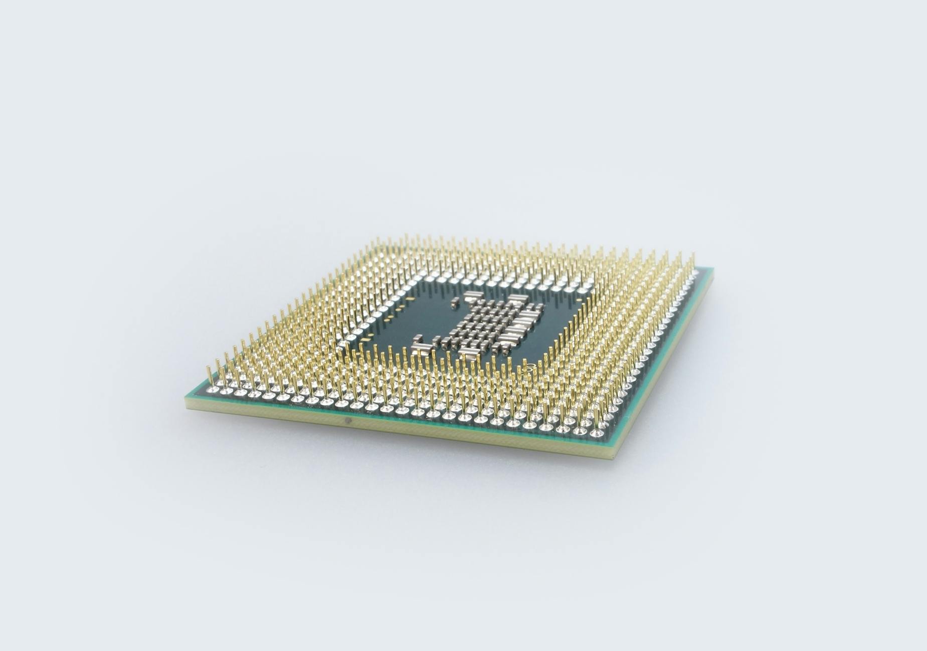
The A2000 is what engineers call a System-on-Chip, or SoC — a single piece of silicon that packs many specialized engines onto one die rather than relying on separate components. It is fabricated at TSMC's 12nm process node, a mature-but-modern manufacturing tier that balances performance, power efficiency and cost. That node choice is telling. It is advanced enough to deliver serious AI throughput, yet practical enough for a first-generation product from a young company that cannot afford the eye-watering costs of bleeding-edge 3nm or 5nm fabrication.
Inside, the chip bundles a custom neural processing unit (NPU) for running machine-learning models, vision processing cores (VPU) for interpreting video, an image signal processor (ISP) for cleaning up camera feeds, dedicated crypto engines for security, and a set of hardware acceleration blocks. The headline feature is the company's patented heterogeneous graph-stream parallel processing architecture — a design approach meant to let these different engines work together efficiently on real-time tasks, rather than passing data back and forth in a way that wastes time and power.

Why "edge AI" is the smart bet
The term edge AI matters here. Most AI we hear about lives in giant data centres — you send a request to the cloud, a server crunches it, and the answer comes back. Edge AI flips that: the intelligence sits inside the device itself, processing data locally without a round trip to the cloud. A smart camera that recognises a number plate on the spot, a drone that avoids obstacles in flight, or a factory sensor that flags a defect instantly — these all need to think on the device, in real time, often without reliable connectivity.
That is exactly the niche the A2000 targets. Netrasemi has positioned it for smart vision devices, surveillance cameras, intelligent video gateways, edge AI boxes, automotive systems, robotics and drones. It is a shrewd choice of battlefield. The data-centre AI accelerator market is dominated by giants like Nvidia, and trying to compete there head-on would be suicidal for a startup. The edge, by contrast, is fragmented, fast-growing and hungry for chips that deliver strong AI performance within tight power and cost budgets — precisely the kind of problem a focused, lean team can attack.
The money and the muscle behind it
Building a chip is brutally capital-intensive, and Netrasemi's backers reflect that reality. The company has raised around ₹125 crore, with software major Zoho and Unicorn India Ventures among its key investors. Zoho's involvement is notable; the Chennai-headquartered firm has been steadily expanding into deep-tech and hardware, and its support gives a semiconductor startup both patient capital and credibility.
Government policy played a direct role too. Netrasemi was among the first four startups picked in 2023 for support under MeitY's Design Linked Incentive (DLI) scheme, receiving roughly ₹15 crore. The DLI programme is a deliberately targeted effort to seed homegrown chip design — covering part of the staggering costs of design tools, intellectual property licensing and fabrication. Co-founder and CEO Jyothis Indirabhai has framed the A2000 as going beyond conventional AI integration by pairing proprietary acceleration hardware with domain-specific tuning. The combination of private venture money and public incentive is, in many ways, the template the government hopes to replicate across dozens of startups.
Designed in India, made in Taiwan
There is an important nuance worth being honest about: the A2000 is designed in India, but it is not made in India. The actual wafers are produced at TSMC's foundries in Taiwan, the company that fabricates chips for Apple, Nvidia and most of the industry's biggest names. "Fabless" companies like Netrasemi handle the architecture, logic design, verification and intellectual property, then hand the blueprint to a foundry that owns the multi-billion-dollar manufacturing plants.
This split is the global norm — even American firms like Qualcomm and AMD are fabless — so it is not a failure on India's part. But it underscores where the country still depends on others. India's much-discussed fabrication plants, including the Tata-PSMC project in Gujarat and assembly-and-test facilities elsewhere, are aimed at closing that gap on the manufacturing side. For now, mastering world-class design is the achievable, high-value first step, and the A2000 demonstrates that the design talent exists.
What completing 'silicon bring-up' really means
It is easy to gloss over the phrase "silicon bring-up," but it is the moment that separates a PowerPoint chip from a real one. Bring-up is when the first physical samples come back from the foundry and engineers power them on to confirm the design works as intended — that the cores boot, the memory talks, the interfaces respond and the AI engines compute correctly. Plenty of ambitious chip projects die at exactly this stage, when expensive silicon turns out to be flawed.
Clearing bring-up means the hard, uncertain part is largely behind Netrasemi. What remains is validation, software and ecosystem work, and the long march to volume manufacturing. The company expects commercial-scale production to begin in 2027. That gap between a working sample and chips you can actually buy is normal, but it is also where many startups stumble — turning a successful prototype into a reliable, mass-produced product that customers can build around is its own enormous challenge.
Why this milestone matters beyond one chip
The deeper significance of the A2000 is what it represents for India's tech ambitions. Semiconductors are the foundation of everything from smartphones and cars to defence systems, and supply-chain shocks in recent years exposed how risky it is to depend entirely on a handful of foreign suppliers. A domestic design capability — especially in AI silicon, the most strategically prized category right now — gives India a measure of resilience and a seat at a table it has mostly watched from outside.
There is also a talent and confidence dividend. A successful first chip creates a generation of engineers who have actually shipped silicon, attracts more venture funding into deep tech, and validates the policy experiment. The A2000 will not dethrone any global player, and it would be a mistake to overhype a single product. But milestones like this are how ecosystems are built — one working chip at a time. If Netrasemi can navigate the path to volume production and win real customers, the more important headline may not be the A2000 itself, but the dozen homegrown chips that follow it.
Source: timestech.in


